Date of birth project
Project overview

The purpose of this project is to design circuits using a seven-segment display to show my date of birth- 08/12/00. The project has several constraints- a common cathode seven-segment display must be used, current limiting resistors must be used, k-mapping technique must be used to obtain simplified logic expressions, and at least one segment must be implemented with NAND only or NOR only logic. This report will explain how I implemented this circuit based on my date of birth.
truth table
The purpose of this truth table is to determine what segments of the seven segment display need to be on or off to show my date of birth as I cycle through the binary sequence. This will allow me to figure out the logic expressions and circuits I need to build later in the project.
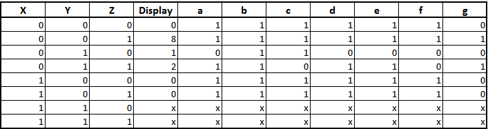
The a-g columns represent each individual LED in the seven segment display. As I toggle the X,Y, and Z inputs on and off in binary order, the seven segment display should show my date of birth - 08/12/00- as shown by the "Display" column. To display these numbers, certain LEDs must be on or off, which is what this table tracks. For example, to display 0, all the LEDs but g must be on. You can see this by following through either of the three rows that are supposed to display a 0. The Xs mean that we don't care what the output is- it has no effect on the LED function. We have these Xs because we only have 6 digits to display, not 8, so the outputs of the last two binary numbers do not matter.
Karnaugh maps & simplified logic expressions
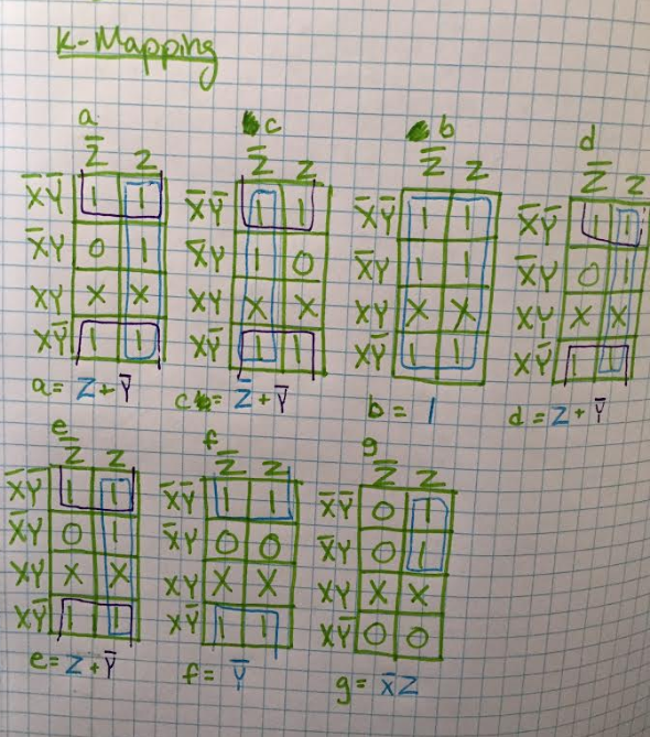
K-Maps work by grouping together like outputs (1s or 0s) to find midterms. K-maps must be filled out in a very specific format. When working with 3 inputs like we did in this project, the 2x4 grid is filled in horizontally with the outputs. For example, the output when the input is 000 in binary, is place in the top left square, and the 001 output is placed in the top right. So the outputs are being placed from left to right and top to bottom. However, the last two rows in the grid are switched. So the 110 and 111 outputs are actually in the third row of the grid, and the 100 and 101 outputs are in the last row of the grid. One can observe this by comparing my K-maps to my truth table. There is also a specific way the K-maps must be labeled- the first two terms go down the side of the K-map and the last term goes across the top. Also the pattern for labeling the specific inputs is as follows- both terms are off, then only the first term is off, both terms are on, and finally only the last term is off. Along the top going horizontally, the term is off and then the term is off. This can be observed in all of my K-maps. In K-maps, terms are grouped in groups of 2, 4, or 8 adjacent, similar terms. There are also methods where one can group four corners of similar outputs, or group between the far left and right or top and bottom outputs (called pac-man). To find the expressions based on these groupings, the common term between all of the inputs in one group are added with the common terms between all of the inputs in the other groups of the map. This creates expressions in Sum of Products form. K- mapping is faster and more procedural than Boolean Algebra, meaning that people are less likely to make mistakes when finding the expressions. This is especially helpful during a project like this when I had to find many expressions so I could create a circuit for each individual segment in the seven-segment display.
Multisim implementation
The image below shows the MultiSim implementation of my seven-segment display. It shows the individual circuits needed to make each segment of the seven-segment display work at the appropriate times to show my date of birth.
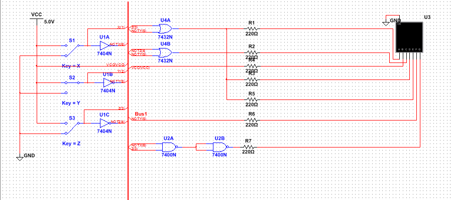
In this circuit, I used bus form because it is easy to implement in MultiSim. In this circuit I used 3 inverter gates (74LS04), 2 OR gates (74LS32), and 2 NAND gates (74LS00). This results in a total of 3 chips- 1 inverter, 1 OR, and 1 NAND, as there are 6 gates in each inverter chip and 4 gates in each OR and NAND chip. I used NAND gates in the circuit for segment G because it was very easy to implement because the logic expression for G was NOTX times Z. To multiply two terms in a circuit, only 2 NAND gates are needed, which is simple and cost effective, compared to using 3 NOR gates, although it is not more efficient then using a single AND gate. However, either way I implemented the G circuit, an extra chip would still be necessary because up until that point I had only used inverter and OR gates.
A seven-segment display shows specific numbers when individual LED segments are on(1)or off(0) depending on what type of display is used. Common Cathode displays, which is what was used in this project, are already connected to ground, so segments need to have a 1 output for the LED to light up. On the other hand, Common Anode displays are already connected to power, so 0 outputs are needed to complete a circuit and turn the LED on. We are using a Common Cathode in this project because it is easier to understand the concept of an LED being on when the circuit has an output of 1, as an output of 0 to turn the LED on
A seven-segment display shows specific numbers when individual LED segments are on(1)or off(0) depending on what type of display is used. Common Cathode displays, which is what was used in this project, are already connected to ground, so segments need to have a 1 output for the LED to light up. On the other hand, Common Anode displays are already connected to power, so 0 outputs are needed to complete a circuit and turn the LED on. We are using a Common Cathode in this project because it is easier to understand the concept of an LED being on when the circuit has an output of 1, as an output of 0 to turn the LED on
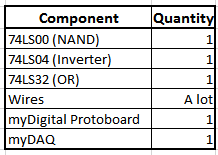
bill of materials
bread-boarding

This picture shows the breadboard before I began wiring my circuits. You can see the seven-segment display in the bottom right corner. Each of those LEDs in the display is controlled by whatever outputs the segments in the DISP1 in the top right corner are connected to.
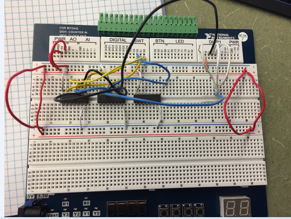
This picture shows my circuit about halfway complete. I have correctly connected the three chips I used to power and ground, and have begun to wire my segments based on my MultiSim implementation. You can see that I have already wired segments a, b, c, and d.
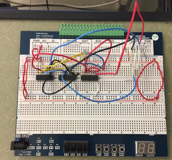
This is the final version of my circuit. I have completely wired all the LEDs based on their logic expressions
My second breadboarding experience went much more smoothly than the first, however I do think it helped that I had very simple circuits to build and that I only needed 3 ICs for the whole project. The major thing I learned was that NOR chips have the opposite input/output layout when compared to other types of ICs. However, this was a skill that I learned from helping my classmates from there projects, because I did not use any NOR chips in my project. I did not have any troubleshooting to do on my project because it worked the first time I tested it.
conclusion
I really enjoyed this project and found that I encountered very few issues. In fact, the only issue I encountered was a mix up between my b and c segment truth tables, which I realized during my breadboarding, but that was very easily remidied by switching my outputs. This project really taught me the usefulness of k- mapping, and how k- mapping is much easier, and results in few mistakes compared to using Boolean Algebra to simplify logic expressions. I also learned to triple check every truth table, k-map, and logic expression before breadboarding, as I both personally experienced, and observed in my classmates, many mistakes made from incorrect tables and k-maps that could have been avoided by double checking answers. I was lucky that my issue had an easy fix, as mentioned above.
extra credit

I found that using NAND gates for segments a,c,d,and e and NOR gates for segments f and g results in the most efficient board, using only 2 chips- one NAND and 1 NOR.
